 | –≠–ª–µ–∫—Ç—Ä–æ–Ω–Ω—ã–π –∫–æ–º–ø–æ–Ω–µ–Ω—Ç: LM32 | –°–∫–∞—á–∞—Ç—å:  PDF PDF  ZIP ZIP |
LM321
Low Power Single Op Amp
General Description
The LM321 brings performance and economy to low power
systems. With a high unity gain frequency and a guaranteed
0.4V/µs
slew
rate,
the
quiescent
current
is
only
430µA/amplifier (5V). The input common mode range in-
cludes ground and therefore the device is able to operate in
single supply applications as well as in dual supply applica-
tions. It is also capable of comfortably driving large capaci-
tive loads.
The LM321 is available in the SOT23-5 package. Overall the
LM321 is a low power, wide supply range performance op
amp that can be designed into a wide range of applications
at an economical price without sacrificing valuable board
space.
Features
(V
CC
= 5V, T
A
= 25∞C. Typical values unless specified).
n
Gain-Bandwidth product
1MHz
n
Low supply current
430µA
n
Low input bias current
45nA
n
Wide supply voltage range
+3V to +32V
n
Stable with high capacitive loads
n
Single version of LM324
Applications
n
Chargers
n
Power supplies
n
Industrial: controls, instruments
n
Desktops
n
Communications infrastructure
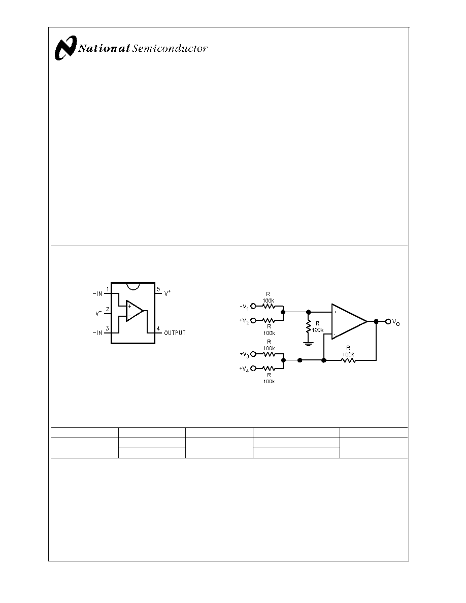
Connection Diagram
SOT23-5
20007601
Top View
Application Circuit
DC Summing Amplifier
(V
IN's
0 V
DC
and V
O
V
DC
)
20007607
Where: V
0
= V
1
+ V
2
- V
3
- V
4
, (V
1
+ V
2
)
(V
3
+ V
4
) to keep V
O
>
0 V
DC
Ordering Information
Package
Part Number
Package Marking
Transport Media
NSC Drawing
5-Pin SOT-23
LM321MF
A63A
1k Units Tape and Reel
MF05A
LM321MFX
3k Units Tape and Reel
April 2001
LM321
Low
Power
Single
Op
Amp
© 2001 National Semiconductor Corporation
DS200076
www.national.com
Absolute Maximum Ratings
(Note 1)
If Military/Aerospace specified devices are required,
please contact the National Semiconductor Sales Office/
Distributors for availability and specifications.
Differential Input Voltage
±
Supply Voltage
Input Current (V
IN
<
-0.3V) (Note 6)
50mA
Supply Voltage (V
+
- V
-
)
32V
Input Voltage
-0.3V to +32V
Output Short Circuit to GND,
V
+
15V and T
A
= 25∞C (Note 2)
Continuous
Storage Temperature Range
-65∞C to 150∞C
Junction Temperature (Note 3)
150∞C
Mounting Temperature
Lead Temp (Soldering, 10 sec)
260∞C
Infrared (10 sec)
215∞C
Thermal Resistance to Ambient (
JA
)
265∞C/W
ESD Tolerance (Note 10)
300V
Operating Ratings
(Note 1)
Temperature Range
-40∞C to 85∞C
Supply Voltage
3V to 30V
Electrical Characteristics
Unless otherwise specified, all limits guaranteed for at T
A
= 25∞C; V
+
= 5V, V
-
=
0V, V
O
= 1.4V. Boldface limits apply at temperature extremes.
Symbol
Parameter
Conditions
Min
(Note 5)
Typ
(Note 4)
Max
(Note 5)
Units
V
OS
Input Offset Voltage
(Note 7)
2
7
9
mV
I
OS
Input Offset Current
5
50
150
nA
I
B
Input Bias Current (Note 8)
45
250
500
nA
V
CM
Input Common-Mode Voltage Range
V
+
= 30V (Note 9)
For CMRR
>
= 50dB
0
V
+
- 1.5
V
+
-2
V
A
V
Large Signal Voltage Gain
(V
+
= 15V, R
L
= 2k
V
O
= 1.4V to 11.4V)
25
15
100
V/mV
PSRR
Power Supply Rejection Ratio
R
S
10k
,
V
+
5V to 30V
65
100
dB
CMRR
Common Mode Rejection Ratio
R
S
10k
65
85
dB
V
O
Output Swing
V
OH
V
+
= 30V, R
L
= 2k
26
V
V
+
= 30V, R
L
= 10k
27
28
V
OL
V
+
= 5V, R
L
= 10k
5
20
mV
I
S
Supply Current, No Load
V
+
= 5V
0.430
0.7
1.15
1.2
mA
V
+
= 30V
0.660
1.5
2.85
3
I
SOURCE
Output Current Sourcing
V
ID
= +1V, V
+
= 15V,
V
O
= 2V
20
10
40
20
mA
I
SINK
Output Current Sinking
V
ID
= -1V
V
+
= 15V, V
O
= 2V
10
5
20
8
mA
V
ID
= -1V
V
+
= 15V, V
O
= 0.2V
12
100
µA
I
O
Output Short Circuit to Ground
(Note 2)
V
+
= 15V
40
85
mA
SR
Slew Rate
V
+
= 15V, R
L
= 2k
,
V
IN
= 0.5 to 3V
C
L
= 100pF, Unity Gain
0.4
V/µs
GBW
Gain Bandwidth Product
V
+
= 30V, f = 100kHz,
V
IN
= 10mV, R
L
= 2k
,
C
L
= 100pF
1
MHz
m
Phase Margin
60
deg
LM321
www.national.com
2
Electrical Characteristics
Unless otherwise specified, all limits guaranteed for at T
A
= 25∞C; V
+
= 5V, V
-
=
0V, V
O
= 1.4V. Boldface limits apply at temperature extremes. (Continued)
Symbol
Parameter
Conditions
Min
(Note 5)
Typ
(Note 4)
Max
(Note 5)
Units
THD
Total Harmonic Distortion
f = 1kHz, A
V
= 20dB
R
L
= 2k
, V
O
= 2V
PP
,
C
L
= 100pF, V
+
= 30V
0.015
%
e
n
Equivalent Input Noise Voltage
f = 1kHz, R
S
= 100
V
+
= 30V
40
nV/
Note 1: Absolute Maximum Ratings indicate limits beyond which damage to the device may occur. Operating Ratings indicate conditions for which the device is
intended to be functional, but specific performance is not guaranteed. For guaranteed specifications and the test conditions, see the Electrical Characteristics.
Note 2: Short circuits from the output V
+
can cause excessive heating and eventual destruction. When considering short circuits to ground the maximum output
current is approximately 40mA independent of the magnitude of V
+
. At values of supply voltage in excess of +15V, continuous short circuits can exceed the power
dissipation ratings and cause eventual destruction.
Note 3: The maximum power dissipation is a function of T
J(MAX)
,
JA
, and T
A
. The maximum allowable power dissipation at any ambient temperature is
P
D
= (T
J(MAX)
- T
A
)/
JA
. All numbers apply for packages soldered directly onto a PC board.
Note 4: Typical values represent the most likely parametric norm.
Note 5: All limits are guaranteed by testing or statistical analysis.
Note 6: This input current will only exist when the voltage at any of the input leads is driven negative. It is due to the collector base junction of the input PNP
transistors becoming forward biased and thereby acting as input diode clamps. In addition to this diode action, there is also lateral NPN parasitic transistor action
on the IC chip. This transistor action can cause the output voltages of the op amps to go to the V
+
voltage level (or to ground for a large overdrive) for the time
duration that an input is driven negative. This is not destructive and normal output states will re-establish when the input voltage, which was negative, again returns
to a value greater than -0.36V (at 25∞C).
Note 7: V
O
1.4V, R
S
= 0
with V
+
from 5V to 30V; and over the full input common-mode range (0V to V
+
- 1.5V) at 25∞C.
Note 8: The direction of the input current is out of the IC due to the PNP input stage. This current is essentially constant, independent of the state of the output so
no loading change exists on the input lines.
Note 9: The input common-mode voltage of either input signal voltage should not be allowed to go negative by more than 0.3V (at 25∞C). The upper end of the
common-mode voltage range is V
+
- 1.5V at 25∞C, but either or both inputs can go to +32V without damage, independent of the magnitude of V
+
.
Note 10: Human Body Model, 1.5k
in series with 100pF.
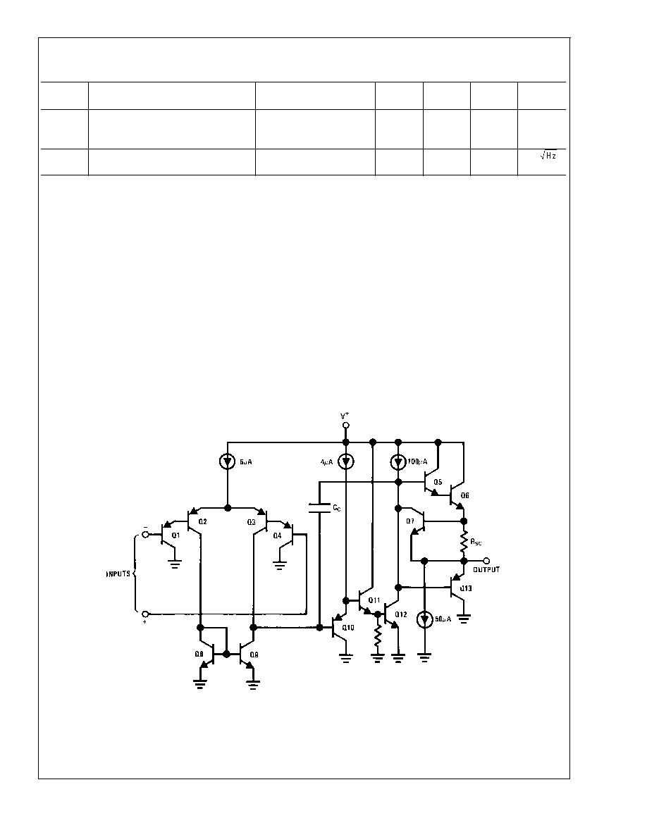
Simplified Schematic
20007603
LM321
www.national.com
3
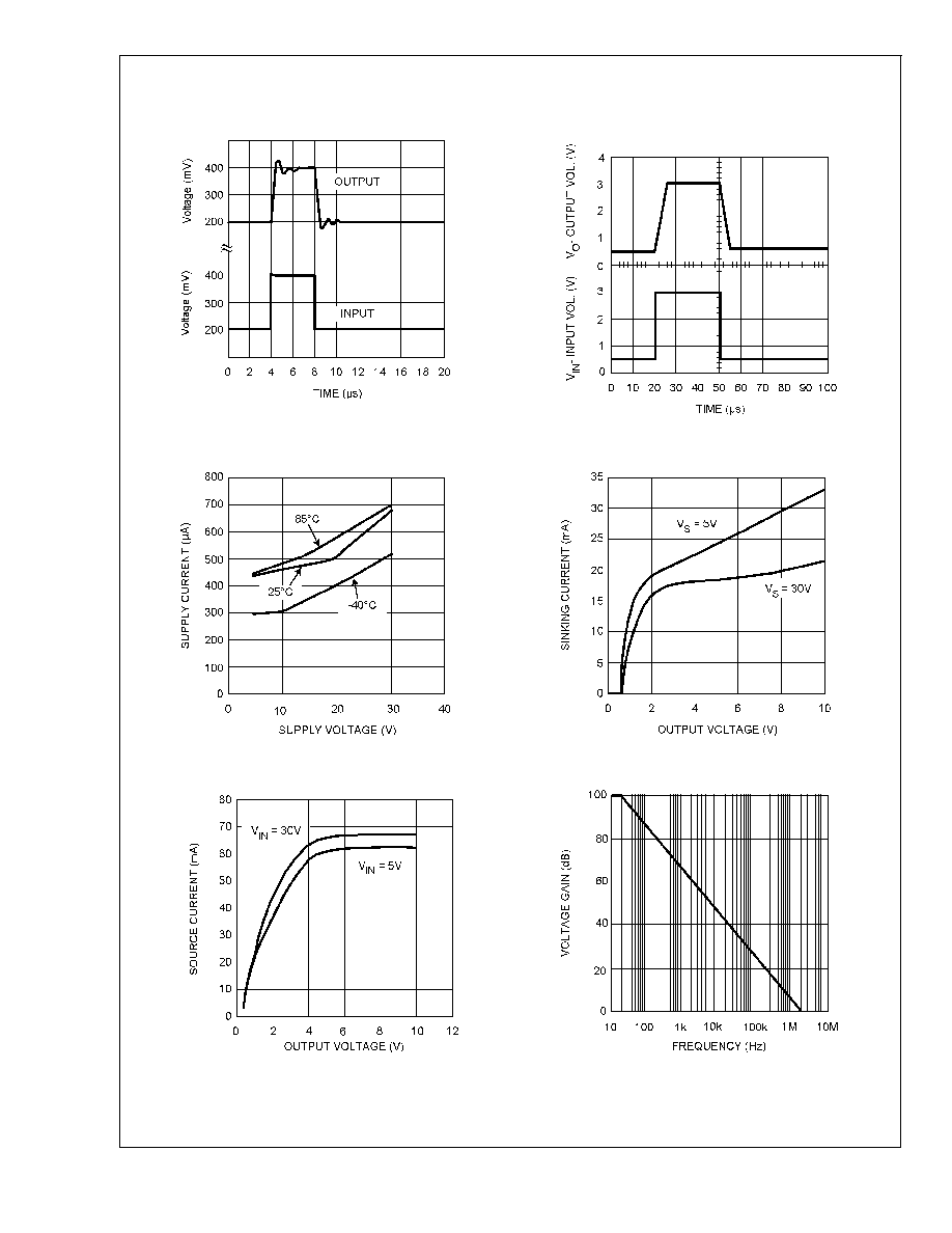
Typical Performance Characteristics
Unless otherwise specified, V
S
= +5V, single supply,
T
A
= 25∞C.
Small Signal Pulse Response
Large Signal Pulse Response
20007604
20007605
Supply Current vs. Supply Voltage
Sinking Current vs. Output Voltage
20007612
20007613
Source Current vs. Output Voltage
Open Loop Frequency Response
20007617
20007614
LM321
www.national.com
4
Application Hints
The LM321 op amp can operate with a single or dual power
supply voltage, has true-differential inputs, and remain in the
linear mode with an input common-mode voltage of 0 V
DC
.
This amplifier operates over a wide range of power supply
voltages, with little change in performance characteristics. At
25∞C amplifier operation is possible down to a minimum
supply voltage of 3V.
Large differential input voltages can be easily accommo-
dated and, as input differential voltage protection diodes are
not needed, no large input currents result from large differ-
ential input voltages. The differential input voltage may be
larger than V
+
without damaging the device. Protection
should be provided to prevent the input voltages from going
negative more than -0.3 V
DC
(at 25∞C). An input clamp diode
with a resistor to the IC input terminal can be used.
To reduce the power supply drain, the amplifier has a class A
output stage for small signal levels which converts to class B
in a large signal mode. This allows the amplifiers to both
source and sink large output currents. Therefore both NPN
and PNP external current boost transistors can be used to
extend the power capability of the basic amplifiers. The
output voltage needs to raise approximately 1 diode drop
above ground to bias the on-chip vertical PNP transistor for
output current sinking applications.
For AC applications, where the load is capacitively coupled
to the output of the amplifier, a resistor should be used, from
the output of the amplifier to ground to increase the class A
bias current and to reduce distortion.
Capacitive loads which are applied directly to the output of
the amplifier reduce the loop stability margin. Values of 50pF
can be accommodated using the worst-case non-inverting
unity gain connection. Large closed loop gains or resistive
isolation should be used if large load capacitance must be
driven by the amplifier.
The bias network of the LM321 establishes a supply current
which is independent of the magnitude of the power supply
voltage over the range of from 3 V
DC
to 30 V
DC
.
Output short circuits either to ground or to the positive power
supply should be of short time duration. Units can be de-
stroyed, not as a result of the short circuit current causing
metal fusing, but rather due to the large increase in IC chip
dissipation which will cause eventual failure due to exces-
sive junction temperatures. The larger value of output source
current which is available at 25∞C provides a larger output
current capability at elevated temperatures than a standard
IC op amp.
The circuits presented in the section on typical applications
emphasize operation on only a single power supply voltage.
If complementary power supplies are available, all of the
standard op amp circuits can be used. In general, introduc-
ing a pseudo-ground (a bias voltage reference of V
+
/2) will
allow operation above and below this value in single power
supply systems. Many application circuits are shown which
take advantage of the wide input common-mode voltage
range which includes ground. In most cases, input biasing is
not required and input voltages which range to ground can
easily be accommodated.
Typical Applications
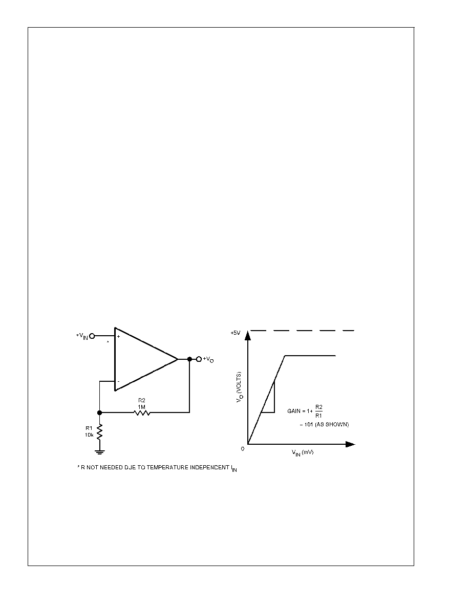
Non-Inverting DC Gain (0V Input = 0V Output)
20007606
LM321
www.national.com
5